


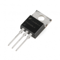
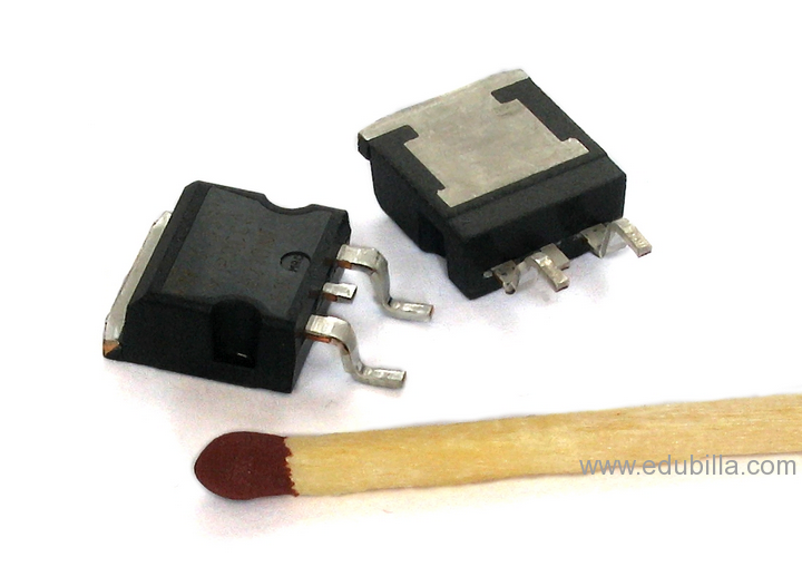
The metal–oxide–semiconductor field-effect transistor is a type of transistor used for amplifying or switching electronic signals.
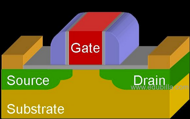
Although the MOSFET is a four-terminal device with source (S), gate (G), drain (D), and body (B) terminals,the body (or substrate) of the MOSFET is often connected to the source terminal, making it a three-terminal device like other field-effect transistors. Because these two terminals are normally connected to each other (short-circuited) internally, only three terminals appear in electrical diagrams. The MOSFET is by far the most common transistor in both digital and analog circuits, though the bipolar junction transistor was at one time much more common.
Dr. Robert W. Bower most notable contribution, however, is his field-effect device with insulated gates—also known as a self-aligned-gate MOSFET (metal–oxide–semiconductor field-effect transistor), or SAGFET. Bower patented this design in 1969 while working at the Hughes Research Laboratories in Malibu, California.
The basic principle of this kind of transistor was first patented by Julius Edgar Lilienfeld in 1925.Twenty five years later, when Bell Telephone attempted to patent the junction transistor, they found Lilienfeld already holding a patent, worded in a way that would include all types of transistors. Bell Labs was able to work out an agreement with Lilienfeld, who was still alive at that time (it is not known if they paid him money or not).It was at that time the Bell Labs version was given the name bipolar junction transistor, or simply junction transistor, and Lilienfeld's design took the name field effect transistor.
In 1959, Dawon Kahng and Martin M. (John) Atalla at Bell Labs invented the metal–oxide–semiconductor field-effect transistor (MOSFET) as an offshoot to the patented FET design.Operationally and structurally different from the bipolar junction transistor,the MOSFET was made by putting an insulating layer on the surface of the semiconductor and then placing a metallic gate electrode on that. It used crystalline silicon for the semiconductor and a thermally oxidized layer of silicon dioxide for the insulator. The silicon MOSFET did not generate localized electron traps at the interface between the silicon and its native oxide layer, and thus was inherently free from the trapping and scattering of carriers that had impeded the performance of earlier field-effect transistors. Following the development of clean rooms to reduce contamination to levels never before thought necessary, and of photolithography and the planar process to allow circuits to be made in very few steps, the Si–SiO2 system possessed such technical attractions as low cost of production (on a per circuit basis) and ease of integration. Largely because of these two factors, the MOSFET has become the most widely used type of transistor in integrated circuits.
Additionally, the method of coupling two complementary MOSFETS (P-channel and N-channel) into one high/low switch, known as CMOS, means that digital circuits dissipate very little power except when actually switched.
The earliest microprocessors starting in 1970 were all "MOS microprocessors"—i.e., fabricated entirely from PMOS logic or fabricated entirely from NMOS logic. In the 1970s, "MOS microprocessors" were often contrasted with "CMOS microprocessors" and "bipolar bit-slice processors".


")


